Welcome to AbrasivesHub.com, your go-to resource for everything related to abrasives and polishing technologies. Today, we delve into the intricate process of wafer polishing, a critical step in semiconductor manufacturing. Whether you’re a seasoned professional or a curious enthusiast, this guide will provide a detailed overview of wafer polishing, its importance, and the techniques involved.
What is Wafer Polishing?
Wafer polishing, also known as Chemical Mechanical Polishing (CMP), is a process used to smooth and flatten the surface of semiconductor wafers. This step is essential in the fabrication of integrated circuits (ICs) and other semiconductor devices. The goal is to achieve a mirror-like finish, free from imperfections and irregularities, which is crucial for the subsequent photolithography and etching processes.
Why is Wafer Polishing Important?
- Surface Flatness and Smoothness: Polishing ensures that the wafer surface is flat and smooth, which is vital for the precise layering of circuits.
- Defect Removal: The process eliminates surface defects such as scratches, pits, and contaminants, which can affect the performance and yield of semiconductor devices.
- Thickness Uniformity: Polishing helps achieve uniform wafer thickness, critical for device performance and reliability.
- Enhanced Performance: A polished wafer surface improves the electrical properties of the semiconductor devices, leading to better performance and efficiency.
The Wafer Polishing Process
The wafer polishing process involves several steps, each crucial for achieving the desired surface quality. Let’s break down these steps:
1. Slicing
The process begins with slicing the monocrystalline ingot into thin wafers using a diamond wire saw. The thickness of these wafers is typically around 1mm.
2. Lapping
Lapping is a mechanical process that uses an abrasive slurry to remove saw marks and achieve a flat surface. This step reduces the wafer thickness and improves surface parallelism.
3. Etching
Chemical etching follows lapping to remove any subsurface damage caused by the mechanical process. This step uses chemical solutions to dissolve a thin layer of the wafer surface, further smoothing it.
4. Polishing
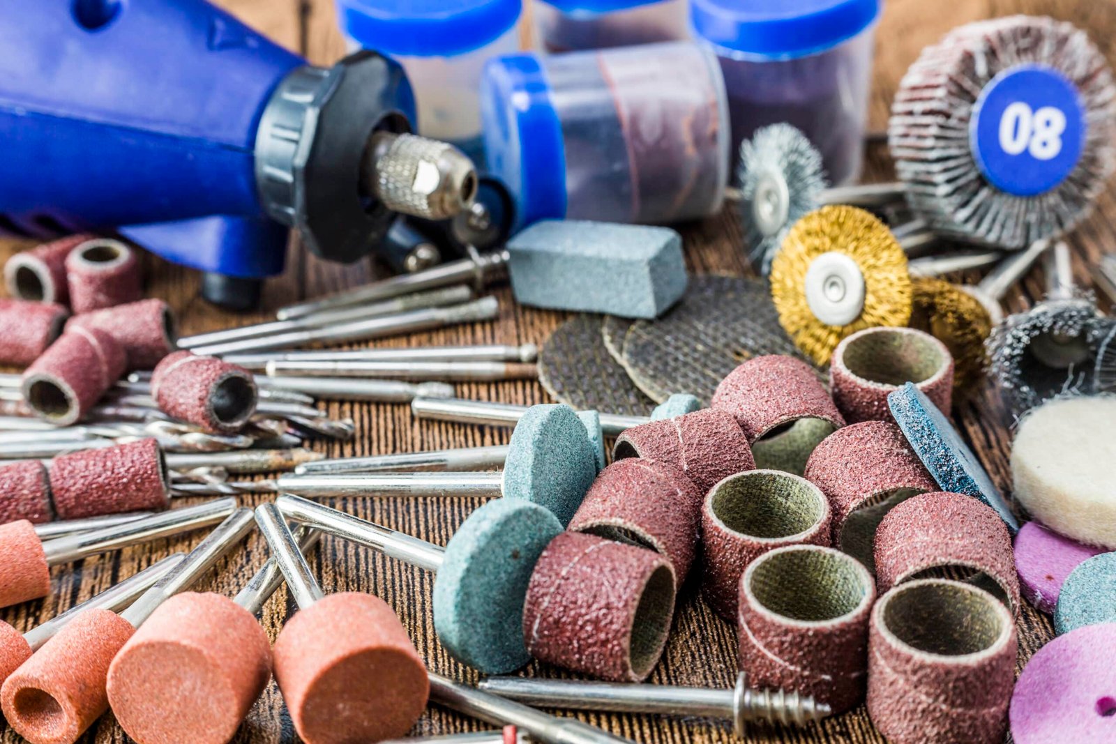
Polishing is the final step in the wafer preparation process. It involves the use of a polishing pad and a chemical slurry to achieve a mirror-like finish. The slurry typically contains fine abrasive particles suspended in a chemical solution.
Types of Wafer Polishing
There are two primary types of wafer polishing: single-side polishing (SSP) and double-side polishing (DSP).
Single-Side Polishing (SSP)
In SSP, only one side of the wafer is polished at a time. This method is commonly used for wafers that require high surface quality on one side, such as those used in MEMS devices.
Double-Side Polishing (DSP)
DSP involves polishing both sides of the wafer simultaneously. This method is preferred for wafers that require high flatness and parallelism on both sides, such as those used in advanced semiconductor devices.
Chemical Mechanical Polishing (CMP)
CMP is the most widely used wafer polishing technique, combining chemical and mechanical processes to achieve the desired surface quality. Here’s a closer look at the CMP process:
CMP Slurry
The CMP slurry is a critical component of the polishing process. It contains abrasive particles, such as silicon dioxide or cerium oxide, suspended in a chemical solution. The slurry’s chemical composition is tailored to react with the wafer material, aiding in the removal of surface material.
Polishing Pads
Polishing pads are made from materials like polyurethane and are designed to provide the right balance of hardness and flexibility. The pad’s surface texture and porosity play a significant role in the polishing performance.
CMP Process Steps
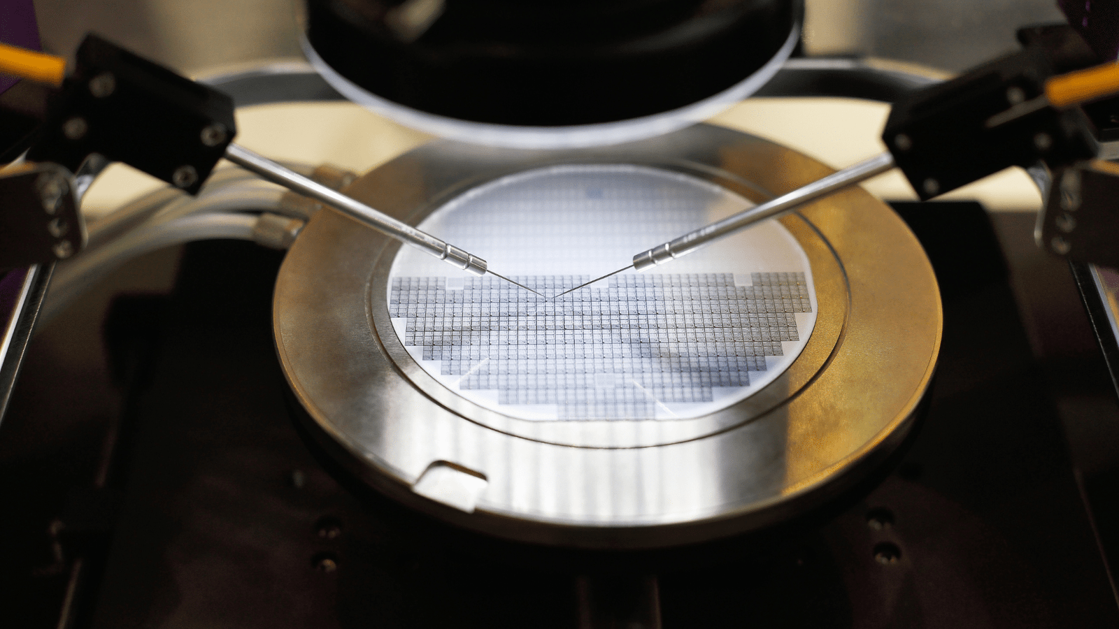
- Wafer Mounting: The wafer is mounted on a carrier, which holds it in place during polishing.
- Slurry Application: The CMP slurry is applied to the polishing pad, which is in contact with the wafer surface.
- Polishing: The wafer and pad are pressed together and rotated, allowing the abrasive particles in the slurry to remove material from the wafer surface.
- Cleaning: After polishing, the wafer is thoroughly cleaned to remove any residual slurry and contaminants.
Challenges and Solutions in Wafer Polishing
Wafer polishing is a complex process with several challenges that need to be addressed to achieve optimal results:
1. Defect Control
Surface defects such as scratches and pits can significantly impact the performance of semiconductor devices. Using high-quality polishing pads and slurries, along with precise process control, helps minimize defects.
2. Uniformity
Achieving uniform thickness and surface quality across the entire wafer is essential. This requires careful optimization of polishing parameters and equipment calibration.
3. Contamination
Contamination from residual slurry and particles can lead to defects and yield loss. Thorough cleaning and inspection after polishing are crucial to ensure a contamination-free surface.
Advancements in Wafer Polishing
The semiconductor industry continually seeks advancements in wafer polishing technologies to meet the demands of smaller and more complex devices. Some recent advancements include:
- Advanced Slurries: Development of slurries with improved chemical formulations and abrasive particles for better polishing performance.
- Automated Polishing Equipment: Use of automated systems with precise process control and monitoring for consistent, high-quality results.
- In-Situ Monitoring: Implementation of in-situ monitoring techniques to provide real-time feedback and control during the polishing process.
Conclusion
Wafer polishing is a critical step in semiconductor manufacturing, ensuring the surface quality and specifications required for high-performance devices. By understanding the process, techniques, and challenges involved, manufacturers can achieve optimal results and meet the demands of the ever-evolving semiconductor industry.
At AbrasivesHub.com, we are committed to providing you with the latest information and resources on wafer polishing and other abrasive technologies. Stay tuned for more in-depth articles and guides to help you stay ahead in the world of semiconductor manufacturing.